Noise Control in Semiconductor Chip Manufacturing and Wafer Inspection Equipment
Semiconductor chip manufacturing and wafer inspection equipment operate in highly precise and controlled environments. Noise generated by these systems can disrupt sensitive processes, compromise product quality, and affect operator well-being. This article examines the noise challenges in semiconductor manufacturing and demonstrates how advanced thermal-acoustic materials can deliver effective solutions.
The Challenges of Noise in Semiconductor Manufacturing
Industry references such as the Semiconductor Manufacturing Handbook by Hwaiyu Geng emphasize that environmental control—including vibration and acoustic stability—is fundamental to maintaining precision, yield, and equipment reliability in advanced semiconductor fabrication. Noise and vibration are not isolated comfort issues; they are tightly linked to process control and measurement accuracy across the fab.
- High-Precision Processes
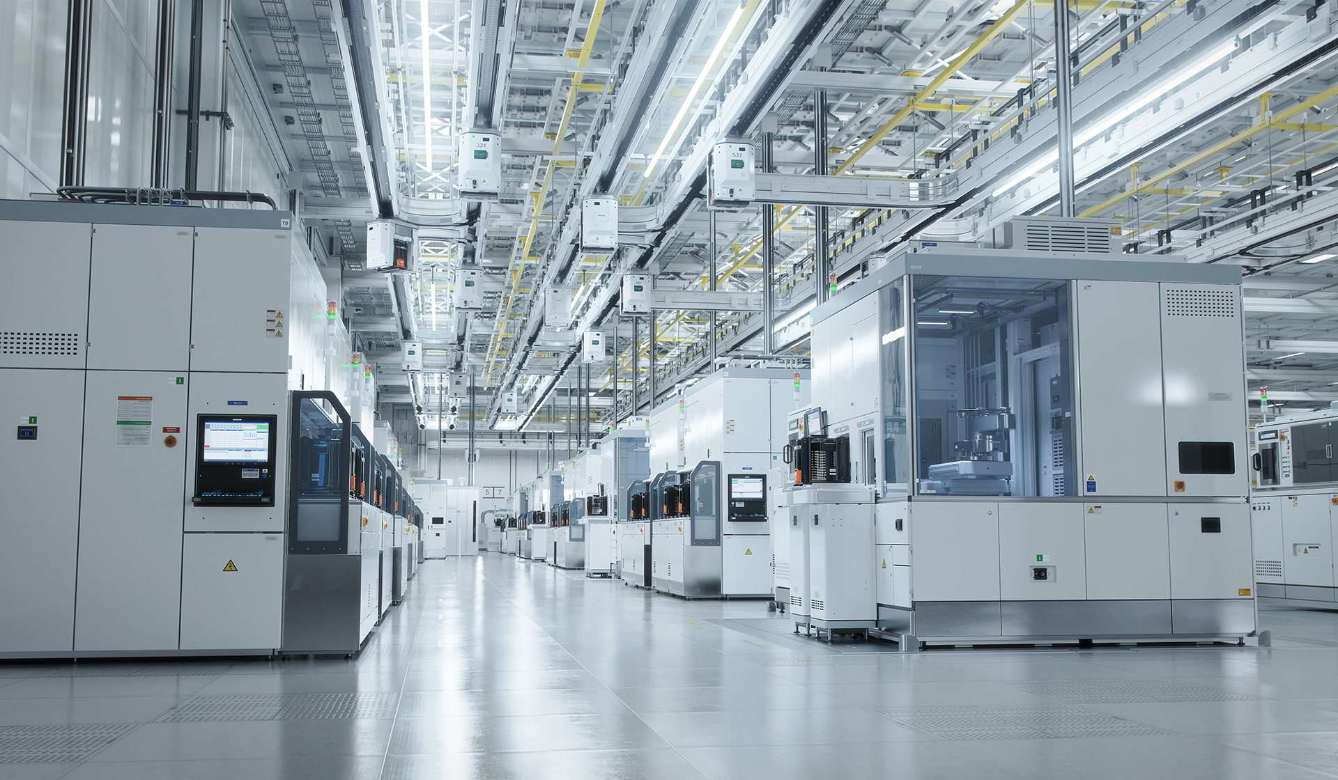
Semiconductor manufacturing involves intricate processes that are highly sensitive to environmental disturbances, including airborne noise and structure-borne vibration. As outlined in industry literature, even low-level vibration can impact lithography alignment, metrology accuracy, and defect detection during wafer inspection. - Complex Machinery
Equipment such as photolithography systems, etchers, deposition tools, and wafer handlers generate noise through high-speed motion systems, vacuum pumps, motors, and turbulent airflow. These sources can excite structural resonances within tool frames, enclosures, and facility floors. - Clean Room Environment
Clean room standards impose strict limits on particulates, outgassing, and material compatibility. The Semiconductor Manufacturing Handbook highlights the challenge of integrating environmental controls without compromising cleanliness, making material selection for acoustic and vibration mitigation especially critical. - Operator Health and Focus
While process integrity is paramount, sustained exposure to elevated noise levels can also affect operator concentration and communication throughout the fab (including clean rooms), increasing the risk of handling errors or delayed response to process deviations. According to an article in Semiconductor Digest, “Turn down that cleanroom!”, some clean rooms can have noise levels at or above 100 dB(A). - Regulatory and Industry Standards
Noise and vibration limits are increasingly considered alongside other environmental specifications in fab design and equipment qualification. Addressing these factors early helps OEMs and fabs align with industry best practices and long-term operational stability. - Yield Risks
Environmental disturbances like noise and vibration can impact yield with issues like alignment drift, measurement uncertainty, and repeatability issues.
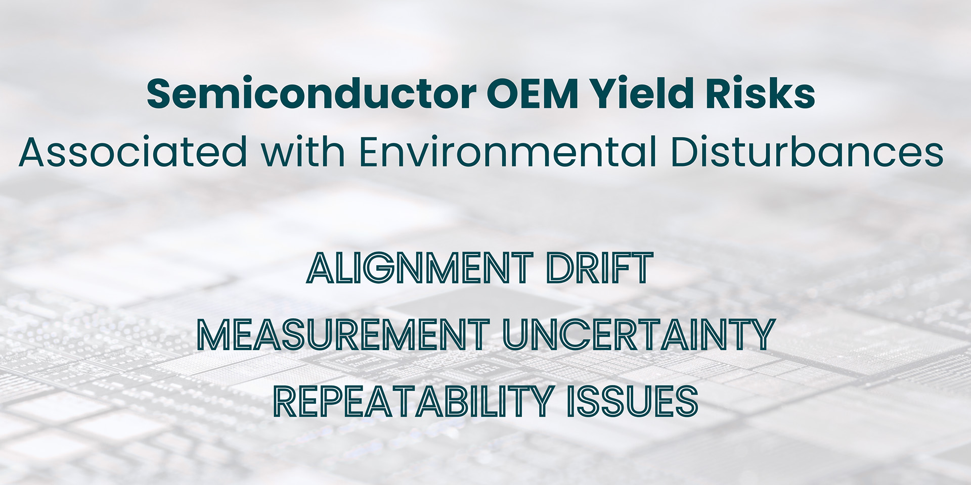
Yield risks from environmental disturbances.
How Thermal-Acoustic Materials Solve Noise Challenges
- Absorptive Open-Cell Foams
Open-cell foams are ideal for absorbing airborne noise generated by machinery and airflow systems. These materials can be incorporated into equipment enclosures and facility walls to minimize sound levels. - Barrier Materials for Sound Blocking
Barrier materials effectively block noise transmission between machinery and adjacent areas, preserving the controlled environment required for precision operations. - Damping Materials for Vibration Control
Damping materials reduce structure-borne noise by isolating vibrations at their source, particularly in high-speed motors and wafer handling systems. - Laminated Composite Materials
Combining absorption, blocking, and damping properties, manufactured laminated composites provide a versatile solution for clean room environments. They help ensure both acoustic performance and compliance with contamination standards.
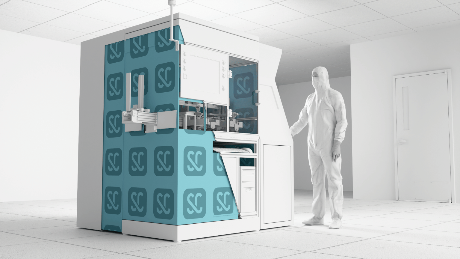
Semiconductor OEM testing equipment with Soundcoat acoustic foam insulation built into the walls of the unit. Soundcoat © 2024
Future Trends in Noise Control for Semiconductor Manufacturing
As semiconductor demand continues to grow, so does the need for innovative noise control solutions. Lightweight, fiber-free, flame-resistant, non-contaminating materials are becoming essential to meet the unique requirements of fabs and clean room environments.
Conclusion:
Effective noise control is critical for ensuring the precision, efficiency, and safety of semiconductor manufacturing and wafer inspection processes. By leveraging advanced thermal-acoustic materials—such as open-cell foams, barrier materials, damping solutions, and laminated composites—manufacturers can address noise challenges and maintain the integrity of their operations. These solutions contribute to a quieter, more efficient environment that supports the demands of this rapidly expanding industry.